Hardware Design
Recommended Minimum System Design
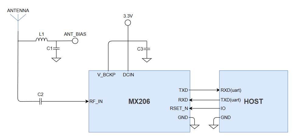
Figure 3-1[]{#_Toc18334 .anchor} MX206 Recommended Minimum System Design
L1 Inductor: Recommended 0603 package, 68nH RF inductor
C1 Capacitor: Recommended two capacitors (100nF and 100pF) in parallel
C2 Capacitor: Recommended 100pF
C3 Capacitor: Recommended multiple 10μF capacitors in parallel with one 100nF capacitor, total capacitance not less than 30μF
Antenna Feeding Design
The MX206 module does not have an internal antenna feeding function, so the antenna feeding must be provided by an external circuit. When designing this external feeding circuit, high-voltage-resistant and high-power components should be preferred. In addition, to enhance the system's protection against lightning strikes and power surges, it is recommended to add protective devices such as gas discharge tubes, varistors, and TVS diodes in the feeding path.
It is strictly prohibited to share the same power supply for ANT_BIAS and the module\'s VCC. Overvoltage/surge introduced from the antenna port will directly impact the main power supply through this path, causing module damage.
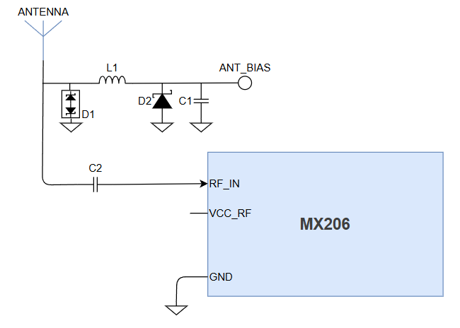
Figure 3-2[]{#_Toc8752 .anchor} MX206 External Antenna Feeding Reference Circuit
L1 (Feeding Inductor): Recommended 0603 package, 68nH RF inductor
C1 (Decoupling Capacitor): Recommended two capacitors (100nF/100pF) in parallel
C2 (DC Blocking Capacitor): Recommended 100pF DC blocking capacitor
D1 (ESD Diode): Should select an ESD protection device supporting high-frequency signals (above 2000MHz)
D2 (TVS Diode): Select a TVS tube with qualified clamping characteristics according to feeding voltage, antenna voltage resistance and other indicators
[!] It is not recommended to use VCC_RF as ANT_BIAS to feed the antenna (due to the limitation of module size, VCC_RF is not equipped with lightning strike protection, surge protection, or overcurrent protection)
Module Power-On and Power-Off
The undershoot and ringing of the module's VCC power-on must be less than 5%VCC, and the power-on time interval must be greater than 500ms.
The undershoot and ringing of the module's V_BCKP power-on must be less than 5%VCC, and the power-on time interval must be greater than 500ms.
Heat Dissipation and Grounding
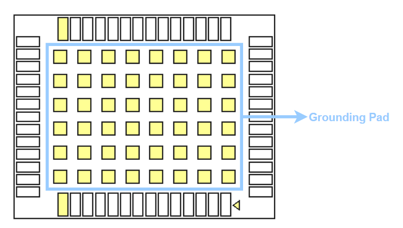
Figure 3-3[]{#_Toc15857 .anchor} MX206 Grounding and Heat Dissipation Pads
The central area at the bottom of the MX206 module is equipped with 48 pads arranged in a matrix. These pads have dual functions of electrical grounding and mechanical heat dissipation. In the PCB layout design, all these pads must be connected to the large-area grounding copper foil area inside or at the bottom of the PCB. The purpose is to use the copper layer of the PCB as an extended heat dissipation surface to form an effective heat conduction path, thereby significantly improving the heat dissipation performance of the module.
Heat Dissipation and Grounding
It is recommended that the PCB pad size of MX206 be the same as the module pad size. For module dimension parameters, refer to 2.3 Mechanical Dimensions.
[!] Appropriate test points can be reserved on the signals of each functional pin of the module to facilitate later hardware debugging and testing.
[!] The PCB pad size design can be optimized according to the customer's production process requirements to ensure manufacturability and reliability during production.